

 Print
PrintWhat designers should expect from a manufacturing partner
Designing micro-optical components is different from designing “small plastic parts.” You’re designing for physics. Light responds to surfaces, edges, alignment features, and material behavior in ways that mechanical intuition alone doesn’t always predict. At micro scale, tiny deviations don’t just shift a dimension, they can change coupling efficiency, scatter, wavefront error, or thermal drift. That’s why the manufacturing partner you choose matters as much as the optical design itself.
This article is a practical guide to what optical designers should expect from an injection molding partner when the parts are truly optical: lens arrays, coupling features, micro-structured light guides, alignment frames, and packaging components that must hold tight positional relationships over time. I’ll focus on the real friction points we see in program, where projects stall, where prototypes mislead, and where “manufacturable” can mean different things depending on who’s speaking.
Precision that matches design intent
In micro-optics, the usual manufacturing trade-offs get compressed. In many products, you can hide a tolerance issue with assembly or calibration. In optics, you often can’t. Once a surface deviates or a datum shifts, the system sees it immediately.
A serious micro-optic molding partner should be able to discuss (in plain language) how they routinely manage:
- Surface quality appropriate to your optical function (not just “smooth,” but measurable and relevant to your wavelength and application)
- Form accuracy that aligns with your optical budget (and doesn’t drift between cavities or lots)
- Positional tolerances on critical alignment features, often where the real optical performance is won or lost
This isn’t a request for magic. It’s a request for clarity. The best partners translate optical requirements into manufacturing controls: tool design choices, gating strategy, material behavior, process windows, and inspection plans. And they will tell you early where the design is robust, and where it’s fragile.
A process built for optical integrity, not “general molding”
Optical parts have a different definition of “damage.” A small scuff, particulate, or handling mark that would be irrelevant on a non-optical component can create scatter, distort a beam, or degrade image quality. So, the conversation needs to move beyond the press and into the environment and handling method:
- Cleanroom molding and controlled handling should be available when your surfaces and features demand it.
- Packaging engineered for optics should be treated as part of the manufacturing process, not an afterthought.
In practice, “clean” isn’t a single standard, it’s a spectrum. Some optics need tight particulate control throughout molding, inspection, and packaging. Others need controlled handling only after molding. A good partner helps you choose the appropriate level of control so you’re not paying for cleanliness you don’t need, or skipping cleanliness you do.
This is one area where Accumold has invested notably, ISO Class 7 and Class 8 cleanroom production options, along with handling and packaging practices designed to protect micro-features and surfaces. That capability is most valuable when it’s applied thoughtfully, only where the optical function truly demands it.
Metrology that can actually measure what you designed
Few sentences slow a micro-optics program like: “We can’t measure that.” Optical designers deserve better, because if a feature can’t be verified, it can’t be controlled, and if it can’t be controlled, it can’t be scaled.
What to expect:
- In-house vision inspection and metrology capable of resolving micro features and datums.
- Custom fixturing and test methods when off-the-shelf measurement doesn’t match your geometry.
- A measurement strategy that ties back to optical performance, not just dimensional pass/fail.
In optical components, it’s often not enough to know that a nominal dimension is “in spec.” You need to know what that dimension does to alignment, how it stacks with other datums, and how variation translates to performance distribution across a production lot.
This is where a manufacturing partner should think like a designer. What are the functional features, what are the reference features, and what are the don’t-care features? The earlier you agree on this, the faster the program moves.
Materials selected for performance, not convenience
Optical injection molding is fundamentally a materials problem disguised as a geometry problem. Material choice affects:
- Transmission and attenuation at your relevant wavelength
- Birefringence and stress response
- Thermal stability and moisture behavior
- Compatibility with downstream processes (cleaning, bonding, coating, reflow, sterilization)
A partner with real micro-optic experience should be comfortable discussing optical-grade polymers and their tradeoffs (COC, COP, PMMA, PC, PS, acrylics, PEI, and others) based on your use case.
They should also be able to talk about higher-temperature demands (for example, scenarios where assemblies see elevated thermal profiles) without treating it as an edge case.
The key is not simply “we can mold that resin.” The key is “we know how that resin behaves at micro scale, what it tends to do at the gate, how it responds to thin features, what it means for tool polish, and what it implies for long-term dimensional stability.”
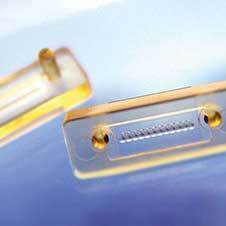
Typical photonics applications where micro molding shines
Micro-optic molding earns its place when you need repeatable micro features at volume and when you want to integrate function into geometry rather than assemble it later. Common application families include:
- Datacom and telecom optics: lens arrays, alignment structures, coupling interfaces, micro housings and frames that control the geometry around fibers and emitters.
- Medical optics: endoscopy-related optical interfaces, diagnostic illumination components, compact imaging assemblies where controlled surfaces and clean handling matter.
- Photonics packaging: parts that hold light sources and sensors in reliable relationship, often under thermal cycling.
- Imaging/projection and sensing: where optical geometry and mechanical packaging must behave as one.
- Light management: micro mirrors, diffractive-like structures, illumination guides and features that shape or distribute light.
Across these, the recurring theme is that molded parts increasingly serve as precision enablers, not just protective housings.
Packaging as an optical operation
If you’ve ever received molded optics that passed inspection but arrived with scuffs, particulates, or rubbed surfaces, you’ve learned this lesson the hard way. Packaging is part of the process. Optical designers should expect a partner to offer packaging options like:
- Trays, gel-paks, and custom carriers that prevent part-on-part contact
- Tape-and-reel where appropriate for automated assembly
- Handling protocols designed to protect critical surfaces and datums
The right packaging approach depends on surface sensitivity, assembly method, and shipping conditions. A good partner will treat this as a design decision, not a logistics decision.
Finishing and downstream needs: coatings, shielding, and surface function
Many optical components don’t stop at “molded.” They require coatings, shielding, or specialized surface properties to perform in the real world. A strong partner will be able to discuss (and coordinate, if appropriate):
- Reflective or anti-reflective coatings
- EMI shielding for optoelectronic environments
- Material approaches for IR performance or high-index needs
Even when finishing is performed by a specialist, the molder’s role matters because finishing success depends on molding decisions such surface prep, tool finish, material selection, and how the part is handled.
What “good partnership” looks like in micro-optic molding
Optical designers are right to be sceptical of polished marketing. The best way to evaluate a manufacturing partner is to watch how they behave around constraints. A partner worth trusting will:
- Ask questions that reveal they understand optical risk (alignment, stress, surface integrity)
- Offer design feedback early, before you pay for tooling that locks in avoidable mistakes
- Tell you what they can measure, how they measure it, and what variability looks like in production
- Help you define what “success” means:, not just passing a drawing, but meeting performance intent
This doesn’t require a sales pitch. It requires competence, transparency, and a shared goal. Getting from prototype to production without compromising the very thing that makes optics work, namely control.
Closing thought
Micro-optic injection molding is where optical ambition meets manufacturing reality. When it works, it gives designers something powerful, freedom. Freedom to integrate optics into compact devices, to scale sophisticated geometries, and to build products where performance is repeatable, not fragile.
And while the goal of this article isn’t to promote any single supplier, I will say this. The organizations that lead in micro-optic molding tend to share the same traits, clean manufacturing options when needed, metrology that keeps up with design, materials depth, and a genuine respect for optical intent. Those are areas where Accumold has built meaningful capability, and they’re exactly what optical designers should expect from any partner they trust with light.