

 Print
PrintAt Photonics West this year, one question came up so often it became a theme: “What materials can you actually use for optical and photonics micro molding?” It’s a fair question, because in optics, material choice isn’t a background detail. It’s often the difference between a design that works beautifully in the lab and one that performs reliably, repeatably, and safely in the field.
Optics and photonics applications are unusual in the way they punish assumptions. Designers may be used to choosing materials based on general mechanical performance, cost, or availability. In photonics, those considerations still matter, but they sit alongside a list of requirements that are far more specific, such as optical transmission at a particular wavelength, birefringence, scattering behavior, thermal drift, moisture uptake, chemical compatibility, cleanliness, and long-term dimensional stability.
Then, to make matters more complex, micro molding adds its own constraints, because a polymer that looks great on a data sheet can behave very differently when you’re trying to fill micro features and hold micron-level tolerances.
This article is a response to that Photonics West question. It’s a practical way to think about materials for molded optics and photonics parts, and what you should expect from a micro molding partner, not only in terms of material range, but in terms of the process command required to turn “a material choice” into dependable end-use performance.
WHAT PHOTONICS DEMANDS FROM MATERIALS
Photonics components are rarely just structural. Even when the polymer isn’t acting as the optical medium, it often determines alignment, stability, and reliability. That means material selection typically needs to account for three broad categories of performance:

1) Optical behavior
If the polymer is in the optical path (lens, light guide, window, micro-structured surface) then transmission, haze, refractive index, and surface fidelity are central. For some applications, the relevant spectrum may be visible. For others, near-IR or IR. The “right” polymer depends on where the system operates and what losses are acceptable.
2) Dimensional and thermal stability
Many optics assemblies are performance-limited by alignment. A few microns of drift due to thermal expansion, relaxation, or humidity effects can show up as coupling loss, beam deviation, or inconsistent sensor response. Materials with predictable thermal behavior and low creep can protect optical function over time.
3) Environmental and regulatory realities
Photonics shows up in medical devices, industrial sensing, aerospace, and communications infrastructure. In many of these, materials must tolerate cleaning agents, sterilization approaches, UV exposure, or long service life. And in safety-critical contexts, you’re not just chasing performance, you’re protecting reliability and reducing risk.
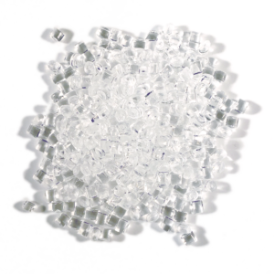
THE “OPTICAL-GRADE” FAMILY
When people ask about materials for optics, they often mean “what can I use that’s clear?” Clarity matters, but it’s only one dimension.
COC and COP (cyclic olefin polymers)
These materials are frequently chosen for optical applications because they offer excellent transparency, low birefringence, low moisture uptake, and strong dimensional stability. They can be highly attractive for microfluidic optics, diagnostic cartridges, lenses in certain regimes, and applications where optical clarity and consistency are critical.
PMMA (acrylic)
PMMA has long been associated with optical clarity and can be an excellent choice in certain imaging and light transmission applications. It can also be sensitive to cracking under certain chemicals or stress conditions, so selection needs to consider the environment the part will see after molding.
Polycarbonate (PC)
PC is a workhorse in many optical and consumer applications because it offers good optical properties alongside toughness and impact resistance. It can be valuable where durability matters, although it may introduce trade-offs in stress birefringence or long-term stability depending on geometry and processing.
The key point is optical polymers are not interchangeable. The best choice often depends on wavelength, allowable haze, surface fidelity requirements, the role of the part (optical path v alignment structure), and the downstream environment.
ENGINEERED THERMOPLASTICS
A surprising number of photonics components are not optical elements themselves, they’re precision structures that hold optical performance in place. In these cases, engineers often prioritize stiffness, thermal performance, and dimensional stability over transparency.
LCP (liquid crystal polymer)
LCP is a compelling choice for high-precision applications because it offers excellent dimensional stability, low moisture absorption, and strong performance in thin-wall geometries, often useful in high-density packaging and connector-related components. It’s frequently considered when tight tolerances and thermal stability are needed.
Ultem (PEI)
PEI can be useful where elevated temperature performance and structural reliability are required, such as in housings or alignment structures near heat-generating components. It’s also a candidate where chemical resistance and long-term stability matter.
PEEK
PEEK is often selected for demanding environments such as high temperature, chemical exposure, and long service life. In photonics contexts, it may appear in components that need to survive harsh conditions or maintain stability in safety-critical systems.
These materials can be harder to mold, especially at micro scale, and they often require more process discipline to achieve both cosmetic and dimensional expectations. But when chosen well and molded well, they can deliver the stability that optical systems depend on.
CAN IT BE MOLDED REPEATABLY?
For optics and photonics, a material choice is only as good as the manufacturing control behind it. Micro molding introduces specific challenges that don’t always show up in conventional injection molding:
- Fill behavior in micro features – tiny ribs, channels, or lens edges can be vulnerable to short shots or incomplete fill if the flow is not managed precisely.
- Stress and birefringence – even clear parts can become optically problematic if residual stress is introduced through processing.
- Surface replication – optical surfaces demand tool finishes and process conditions that protect fidelity.
- Warpage and shrink variation – small variations can create big optical consequences in alignment features and mating geometries.
- Part handling and cleanliness – optical surfaces can be damaged or contaminated easily, making packaging and handling part of the process, not an afterthought.
So, when visitors at the show asked, “What materials do you offer?” the deeper question was “can you control those materials at micro scale in a way that protects optical intent?” That’s what separates a “material list” from a true capability.
WHAT YOU SHOULD EXPECT FROM A MICRO MOLDING PARTNER
A capable micro molder should offer more than a catalogue of resins. You should expect five things:
1) A broad and relevant material toolkit
That includes optical-grade polymers (COC/COP, PMMA, PC) and engineered materials (LCP, PEI/Ultem, PEEK), plus the practical knowledge of where each makes sense.
2) Guidance tied to function, not preference
A good partner asks “Is the polymer in the optical path? Is it a precision alignment structure? What wavelength matters? What is the environmental exposure? What are the tolerance sensitivities?” The goal is to narrow the choice to what supports performance and manufacturability.
3) Process knowledge that accounts for optical risks
Materials behave differently at micro scale. A micro molder should know how gating, flow paths, temperature control, and cycle strategy influence stress, surface quality, and consistency.
4) Metrology that confirms what matters
In photonics, measurement is not just about dimensions. It’s also about verifying the features that affect alignment and optical performance, and monitoring stability across production.
5) Clean handling and packaging options when needed
Optical parts can be compromised after molding. A capable partner supports appropriate handling protocols and packaging approaches to protect surfaces and micro features.
SAFETY-CRITICAL APPLICATIONS
Many optics and photonics components end up in contexts where performance isn’t just “nice to have.” Think medical diagnostics, surgical visualization, aerospace sensing, industrial safety systems, and high-reliability communications. In these environments, a small drift, an unexpected material interaction, or a surface defect can lead to failure modes that are costly, or worse.
That’s why material selection needs to be treated as part of risk management. The “right” polymer is the one that delivers reliable performance under real conditions, not just the one that meets a nominal property at room temperature. And the “right” manufacturing partner is one who understands that the material and the process are inseparable.
CONCLUSION
The question we heard repeatedly at Photonics West “What materials can you use?” is really shorthand for something bigger, namely “Can you help us choose and control materials so our optics will perform in the real world?”
The best outcomes happen when material selection is treated as a system decision looking at optical needs, mechanical stability, environment, manufacturability, and measurement. In micro molding, that joined-up thinking is what turns polymers into performance.
At Accumold, we see material capability as both range and discipline, being able to work across optical-grade and engineered polymers, and applying the process control needed to mold them repeatably at micro scale. That combination is what supports photonics programs as they move from concept to production, especially when the end application demands reliability you can’t negotiate.
If you’re designing molded optics or photonics-enabled assemblies, don’t treat material choice as a last-mile decision. Treat it as the start of manufacturable performance, and choose a partner who can prove they understand what that really means.
This article also appeared on PhotonicsOnline.com in February 2026.